Japan’s NEDO is expected to fund about ¥16 billion of the roughly ¥24 billion project. The line will be located in Iwate Prefecture.
NTT plans to ship commercial samples in 2028, produce 100,000 units a year by 2031, and reach 1 million units a year by 2033.
Furukawa Electric and Shinko Electric are involved in component manufacturing and assembly.
Optical chiplets will sit next to CPUs and GPUs
The devices use NTT’s photonics-electronics convergence, or PEC, technology.
An optical chiplet combines:
- a photonic integrated circuit (PIC);
- an electronic integrated circuit (EIC);
- optical transmitters and receivers;
- high-density packaging.
The CPU or GPU remains electronic. The optical chiplet replaces part of the electrical data path between processors with an optical link.
0.26 pJ/bit and 1 million units a year
NTT has previously shown an optical-chiplet prototype measuring about 8 × 10 mm. The company has cited a target efficiency of around 0.26 picojoules per bit.
| Specification | NTT optical chiplet |
| Technology | Photonics-electronics convergence |
| Main use | CPU/GPU interconnects |
| Prototype size | About 8 × 10 mm |
| Demonstrated signal rate | 64 Gbit/s |
| Target efficiency | About 0.26 pJ/bit |
| Commercial samples | 2028 |
| Production target | 100,000/year by 2031 |
| Longer-term target | 1 million/year by 2033 |
| Manufacturing target | More than 10× higher productivity than current R&D processes |
| Location | Iwate, Japan |
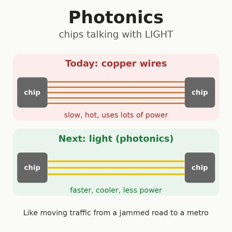
Copper links are becoming a power bottleneck
High-speed electrical links require drivers, equalization and retimers to compensate for signal loss.
That increases power consumption and heat. Optical links can carry high-bandwidth data with lower transmission losses over longer distances.
For AI clusters, this reduces the power used to move data between accelerators.
NTT’s approach is to shorten electrical paths and move more processor I/O into the optical domain.
PEC-3 vs. PEC-2
NTT’s new chiplet belongs to the PEC-3 / IOWN 3.0 generation. The previous PEC-2 generation focused mainly on board-level optical links.
| PEC-2 | PEC-3 | |
| Main connection | Board-to-board | Package-to-package |
| Optical component position | On or around the board | Next to CPU/GPU packages |
| Main goal | Reduce board-level electrical transmission | Reduce processor I/O power |
| Form factor | Optical engines and modules | Optical chiplets |
| Target hardware | Boards and switches | CPUs, GPUs and accelerators |
PEC-3 moves the optical conversion point closer to the processor and reduces the length of high-speed electrical links.

The manufacturing problem
Optical chiplets combine silicon photonics, electronic ICs, compound-semiconductor optical components and advanced packaging.
The partners divide the work as follows:
- NTT Innovative Devices — manufacturing, testing and packaging.
- Japan Semiconductor — silicon-photonics production and heterogeneous integration.
- Furukawa Electric — compound-semiconductor optical components.
- Shinko Electric — packaging and inspection.
The project targets more than a 10× improvement in manufacturing productivity versus current research-stage processes.
Production targets
NTT’s roadmap:
- 2028 — commercial samples
- 2031 — 100,000 units per year
- 2033 — 1 million units per year
That implies a 10× increase in annual output between 2031 and 2033.
Why it matters for AI systems
AI clusters need more bandwidth between processors while data-center power density continues to rise. NTT’s roadmap moves optics progressively closer to the compute silicon:
PEC-1: system-level optical links
- → PEC-2: board-to-board.
- → PEC-3: package-to-package.
- → PEC-4: die-to-die
If PEC-3 reaches mass production, optical I/O could move from external networking hardware directly into CPU and GPU packages.